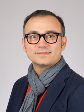
SPEAKER PROFILE |
 Dr. Yasin Ekinci Paul Scherrer Institute Switzerland |
Let's find the nano-defects: Photomask inspection with lensless EUV imaging
Abstract
The tremendous shrinkage of the semiconductor devices in the last five decades, as predicted by Moore’s law, has changed our daily lives. This progress was possible through advancements in photolithography and optical metrology. Extreme ultraviolet (EUV) lithography at 13.5 nm wavelength is the manufacturing method for high-volume semiconductor manufacturing at 7 nm technology node and below. To enable future progress, many challenges lie ahead. One of the challenges of the industry is manufacturing of defect-free masks for which and effective inspection method is missing. In my talk, I will discuss how to overcome these by using lensless EUV imaging.
Bio
Yasin Ekinci is head of the Advanced lithography and Metrology group and acting head of the Laboratory for Micro and Nanotechnology at Paul Scherrer Institute. He obtained his PhD in Max-Planck Institute for Dynamics and Self-Organization, Göttingen, Germany in 2003. He worked on various topics of nanoscience and technology, including atom optics, surface science, EUV lithography, resist materials, coherent scattering, lensless imaging, plasmonics, biosensing, semiconductor nanostructures, and nanofluidics. He is author/co-author of about 190 papers and 5 patent applications. He is a fellow of SPIE.