SPEAKER PROFILE |
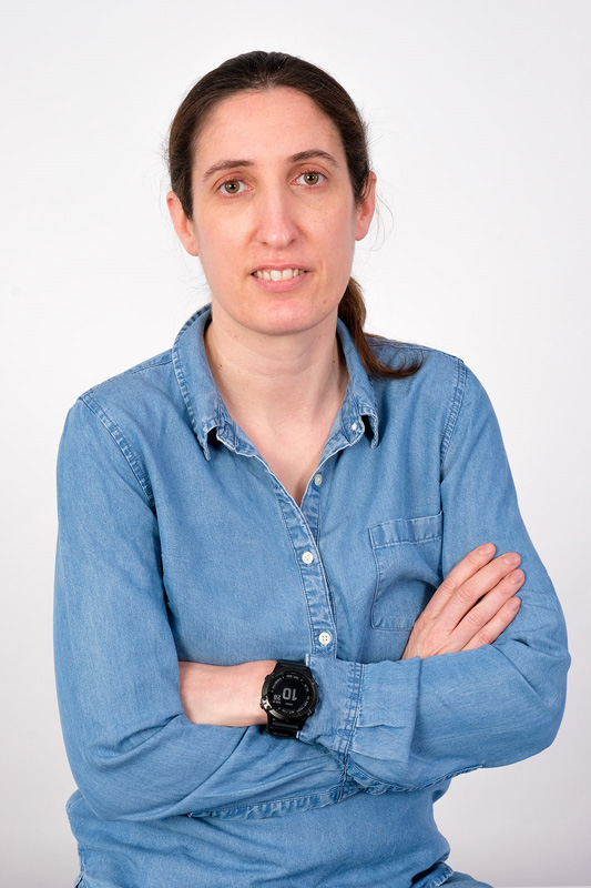
 Dr. Marta Fernandez-Regulez NanoNEMS research group. Instituto de Microelectrónica de Barcelona, IMB-CNM (CSIC), Bellaterra Spain |
Block Copolymers: A Scalable Path to Advanced Semiconductor Devices
Abstract
The continuous miniaturization of semiconductor devices has relied on advancements in micro/nanofabrication techniques. While Extreme UV (EUV) lithography has become the standard for advanced industrial processes, its high costs and complexity have driven interest in alternative, more affordable high-resolution patterning methods. Directed self-assembly (DSA) of block copolymers (BCPs) has emerged as a promising solution, offering sub-10 nm resolution, scalability, and compatibility with high-volume manufacturing. By combining the natural self-assembly properties of BCPs with chemical or topographical guiding patterns, DSA enables the fabrication of nanometric structures with enhanced resolution and throughput.
In this talk, I will present our recent advancements in DSA technologies, including their integration into standard micro/nanofabrication workflows. These developments have enabled the fabrication of functional devices such as suspended nanowires, MEMS/NEMS, and thermoelectric thin films with improved performance. I will also explore the potential of DSA for next-generation applications, such as the fabrication of quantum devices, highlighting its role as a transformative tool for advanced nanofabrication in the semiconductor industry.
In this talk, I will present our recent advancements in DSA technologies, including their integration into standard micro/nanofabrication workflows. These developments have enabled the fabrication of functional devices such as suspended nanowires, MEMS/NEMS, and thermoelectric thin films with improved performance. I will also explore the potential of DSA for next-generation applications, such as the fabrication of quantum devices, highlighting its role as a transformative tool for advanced nanofabrication in the semiconductor industry.
Bio
Marta Fernández-Regúlez is a senior researcher in the NanoNEMS group at IMB-CNM (CSIC) with over 15 years of experience in the development and application of micro and nanotechnologies. She holds a degree in Physics from the University of Valladolid and a PhD in Electronic Engineering from the Autonomous University of Barcelona (2012). Her expertise lies in bottom-up methods for nanofabrication, with a particular focus on directed self-assembly (DSA) of block copolymers for the creation of advanced nanoscale devices. Her research involves the application of these methods to a variety of fields, including semiconductor nano-patterning, nanoelectronics, energy devices and MEMS/NEMS technologies. Through her career, she has conducted a predoctoral stay at the University of Berkeley and postdoctoral research at CEA-LETI, where she closely collaborated with the semiconductor industry on innovative patterning solutions.