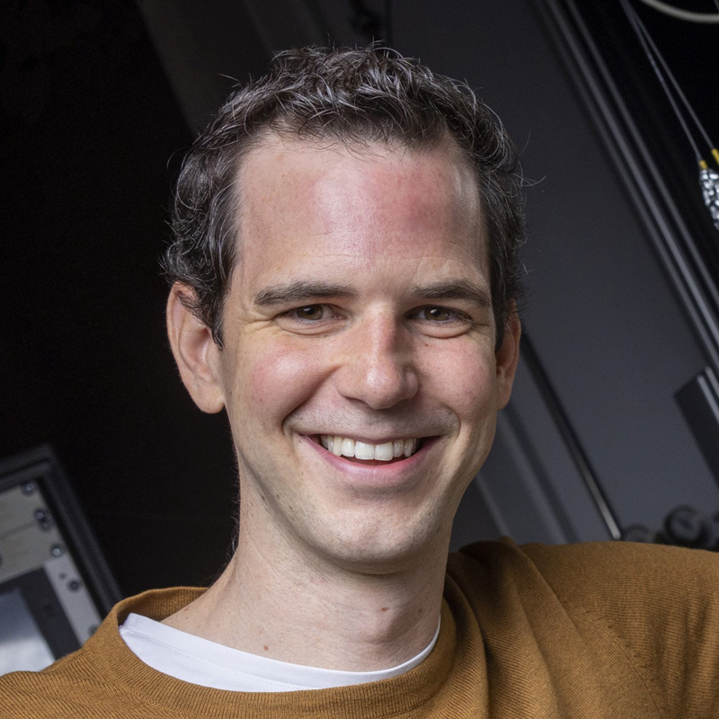
SPEAKER PROFILE |
 Dr. Bruno Schuler nanotech@surfaces Lab, Empa - Swiss Federal Laboratories for Materials Science and Technology Switzerland |
Probing Atomic Defects in 2D Semiconductors with Lightwave-Driven STM
Abstract
Two-dimensional (2D) semiconductors provide an exciting platform to engineer atomic quantum systems in a robust, yet tunable solid-state system. This talk explores the intriguing physics of single point defects in transition metal dichalcogenide (TMD) monolayers, investigated through atomically resolved scanning probe microscopy.
We have determined the layer-dependent charge transfer lifetimes of selenium vacancies in WSe? on graphene substrates, spanning picosecond to nanosecond timescales [1]. By leveraging our recently developed lightwave-driven scanning tunneling microscope (THz-STM) [2,3], we could probe the ultrafast charge dynamics on the atomic scale. Time-domain sampling with a THz pump-THz probe scheme enabled capturing atomic-scale snapshots of transient Coulomb blockade, a hallmark of charge transport mediated by quantized defect states [4].
Moreover, the extended charge state lifetimes provided by hBN decoupling layers facilitated the local, electrical stimulation of excitonic emission from pristine MoS2 and individual charged defects via STM luminescence (STML).
By combining the structural and electronic properties accessible by conventional scanning probe microscopy with the optical fingerprint from STML and the excited-state dynamics revealed through pump-probe THz-STM, we gain a comprehensive microscopic understanding of localized quantum states in low-dimensional materials.
He received his BSc and MSc in Physics from ETH Zurich, and his PhD and postdoctoral research were conducted at the IBM Research Labs in Zurich, where he was awarded the Swiss Physical Society Award in Applied Physics and two IBM Research Division Awards for his pioneering work in chemical structure identification of single molecules using CO-tip noncontact atomic force microscopy. He later worked as an SNF Postdoctoral Fellow and Junior Group Leader at the Lawrence Berkeley National Lab's Molecular Foundry. In 2021, he received an ERC Starting Grant for developing an ultrafast THz-STM for studying the dynamics in 2D materials.
We have determined the layer-dependent charge transfer lifetimes of selenium vacancies in WSe? on graphene substrates, spanning picosecond to nanosecond timescales [1]. By leveraging our recently developed lightwave-driven scanning tunneling microscope (THz-STM) [2,3], we could probe the ultrafast charge dynamics on the atomic scale. Time-domain sampling with a THz pump-THz probe scheme enabled capturing atomic-scale snapshots of transient Coulomb blockade, a hallmark of charge transport mediated by quantized defect states [4].
Moreover, the extended charge state lifetimes provided by hBN decoupling layers facilitated the local, electrical stimulation of excitonic emission from pristine MoS2 and individual charged defects via STM luminescence (STML).
By combining the structural and electronic properties accessible by conventional scanning probe microscopy with the optical fingerprint from STML and the excited-state dynamics revealed through pump-probe THz-STM, we gain a comprehensive microscopic understanding of localized quantum states in low-dimensional materials.
References:
[1] L. Bobzien et al. Phys. Rev. Lett. (accepted), arxiv: 2407.04508
[2] J. Allerbeck et al. ACS Photonics 10, 3888 (2023)
[3] L. Bobzien et al. APL Mater. 12, 051110 (2024)
[4] J. Allerbeck et al. arXiv:2412.13718 (2024)
[5] L. Huberich et al. (in preparation)
[1] L. Bobzien et al. Phys. Rev. Lett. (accepted), arxiv: 2407.04508
[2] J. Allerbeck et al. ACS Photonics 10, 3888 (2023)
[3] L. Bobzien et al. APL Mater. 12, 051110 (2024)
[4] J. Allerbeck et al. arXiv:2412.13718 (2024)
[5] L. Huberich et al. (in preparation)
Bio
Bruno Schuler is the Group Leader of the 2D Quantum Materials Group at the Swiss Federal Laboratories for Materials Science and Technology, interested in exploring low-dimensional quantum materials with cross-correlation microscopy at the ultimate spatial, energy and time resolution.He received his BSc and MSc in Physics from ETH Zurich, and his PhD and postdoctoral research were conducted at the IBM Research Labs in Zurich, where he was awarded the Swiss Physical Society Award in Applied Physics and two IBM Research Division Awards for his pioneering work in chemical structure identification of single molecules using CO-tip noncontact atomic force microscopy. He later worked as an SNF Postdoctoral Fellow and Junior Group Leader at the Lawrence Berkeley National Lab's Molecular Foundry. In 2021, he received an ERC Starting Grant for developing an ultrafast THz-STM for studying the dynamics in 2D materials.